All-in-one PCB prototyping workflow
Rapid turnaround for research teams
Handles multilayer and complex boards
Integrated PCB prototyping workflow
Tracks Laser & Electronics Ltd supports a coordinated PCB prototyping workflow where all stages from design to testing and optimisation can be completed in a single day. We use a connected set of tools, including Tracks ProtoLaser systems, to handle each step in sequence, starting from layout data and moving through production and validation. This approach helps us maintain consistency while keeping the entire process efficient and suitable for rapid development of functional PCB prototypes and multilayer designs. For further details or project enquiries, feel free to contact us.

Software with intuitive operation
CircuitPro guides users through every stage of PCB production, from CAD import to final output. It combines CAM processing and machine control in a single system, automatically detecting connected ProtoMat and ProtoLaser units. Built-in design rule checks, a production wizard, and real-time messaging keep setup simple and errors to a minimum.


PCB Structuring – Fast Circuit Board Fabrication
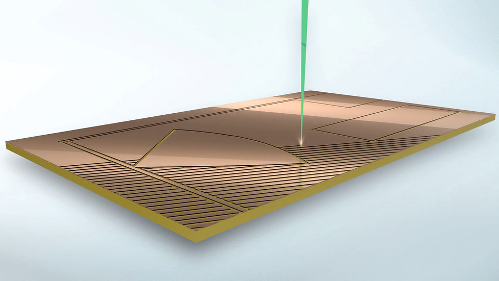
PCB structuring supports rapid in-house fabrication of single-sided, double-sided, multilayer, RF, and flexible boards using mechanical or laser-based methods. Mechanical systems mill precise insulating channels to define conductive tracks, while LPKF ProtoLaser systems deliver faster, more accurate results across advanced materials including ceramics, Duroid, and PTFE.
PCB Drilling
LPKF circuit board plotters and ProtoLaser systems support both mechanical and laser drilling for through-holes and blind vias across single, double, and multilayer boards. Laser drilling achieves microvias below 200 µm on a wide range of substrates, while mechanical drilling offers a cost-effective solution for standard FR4 prototyping from 0.15 mm upwards.


Through-Hole Plating Solutions
Through-hole plating bridges fabrication and full electrical functionality, enabling complete multilayer assemblies. LPKF ProConduct® offers a fast, chemical-free method for metallising vias in a lab-safe environment, while the Contac S4 system uses controlled electrolytic processes for uniform copper deposition in more advanced or production-grade applications.
PCB Cutting and Depaneling Solutions
LPKF ProtoMat and ProtoLaser systems handle board separation directly from the base material using either mechanical milling or laser structuring. Multiple boards can be arranged on a single panel and precisely cut within minutes, supported by integrated parameter libraries and software-assisted panelisation for efficient, accurate depaneling.


SMT and PCB Finishing Solutions
SMT and finishing processes take bare boards through to fully functional assemblies, covering solder paste printing, component placement, and reflow soldering. LPKF systems support fine pitch layouts, RoHS-compliant soldering, and protective solder mask application, with in-house stencil milling and board marking available to keep the entire process fast and self-contained.
Process steps for PCB prototyping made simple
Call us today for PCB prototyping process support.
