
Eight-layer PCB production on site
Micro-material processing for advanced R&D
Seamless workflow from design to testing
Fast, flexible PCB prototyping for every engineering lab
Tracks Laser & Electronics Ltd provides PCB prototyping systems that let you handle every stage of the process in-house, speeding up your research and development. With our solutions, you can go from circuit design to finished prototype in a single day, giving you the freedom to test, iterate, and improve without delays.
Our coordinated methods and tools, including our intuitive CircuitPro system, support everything from basic board structuring to complex multilayer builds. We have helped engineering teams keep projects moving while reducing development costs. Whether you're developing medical devices, aerospace components, or consumer electronics, you stay in control with us.
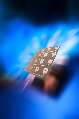
What you gain with our PCB prototyping solutions
-
Complete in-house prototyping from design to optimisation
-
Multilayer board production: up to 8 layers
-
Direct laser processing for medical device research
-
CircuitPro software for step-by-step workflow
-
Micro material processing capabilities in your lab
-
Through-hole plating, cutting, and SMT finishing support
-
Ideal for engineering labs and innovation teams
-
Rapid turnaround to accelerate your R&D cycles

A complete, step-by-step PCB prototyping system
Our systems cover every stage: our intelligent software walks you through data preparation, then our precise equipment handles PCB structuring, drilling, through-hole plating, cutting, depaneling, and SMT finishing. You get all your tools from one source, avoiding compatibility headaches.
Tracks Laser & Electronics Ltd understands the pace of R&D environments, so we’ve designed our process for reliability and speed. With up to eight layers possible on site, your team can tackle increasingly complex designs without sending files or boards to third parties. For more information about our PCB prototyping solutions, contact us today.
