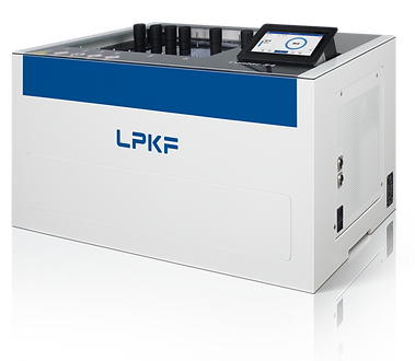
We are serving across UK and Ireland
Automated layer structuring technology
Chemical-free through-hole plating
In-house multilayer PCB manufacturing
Multilayer circuit boards enable the integration of complex electronic functions within a compact design by combining multiple conductive and insulating layers into a single structure. Tracks Laser & Electronics Ltd provides a complete solution for in-house PCB prototyping, supporting the production of up to eight-layer boards within a laboratory environment, including applications in advanced electronics and medical research.
The process involves structured layer creation, lamination with insulating prepregs, and precise through-hole plating for reliable electrical interconnection. Outer layers typically use single or double-sided PCBs, while internal layers form the core circuit architecture. This approach allows efficient prototyping, improved design flexibility, and streamlined development of advanced multilayer electronic systems.
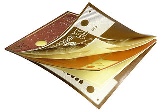
Three steps to multilayer PCB fabrication

Structuring of Traces
Using an LPKF ProtoMat circuit board plotter or ProtoLaser system, circuit traces are structured directly from layout data. Automatic tool change and fiducial camera alignment enable precise, layer-by-layer processing with minimal manual intervention.

Lamination
Structured layers are accurately stacked with prepreg insulating material placed between conductive layers. The MultiPress S4 hydraulic system ensures consistent lamination, delivering stable results even for high-frequency multilayer applications.

Through-Hole Plating
Electrical interconnection between layers is created by drilling vias with a ProtoMat system. ProConduct enables chemical-free conductive connection, while electroplating is recommended for multilayer stacks exceeding four layers.
Systems for In-House Multilayer PCB Production
Structuring
LPKF ProtoMat S104
LPKF ProtoMat systems enable fast, precise and fully in-house PCB prototyping from RF to multilayer applications. Designed for laboratory use, they support automated workflows, high-accuracy machining and complete control from design to finished board.
-
LPKF ProtoMat S104 Overview
A high-end PCB plotter designed for RF and microwave applications, featuring automatic tool change, optical registration, a vacuum table and high-speed spindle operation for maximum precision and repeatability.
-
Fully Automatic Operation
Sensor-based measurement of material and copper thickness ensures accurate milling depth calculation. Automatic tool switching across 20 positions enables uninterrupted production with minimal user input.
-
High-Precision Machining
With spindle speeds up to 100,000 rpm and granite base stability, the system delivers fine structural detail, consistent milling channels and high repeat accuracy for complex PCB designs.
-
2.5D Machining Capability
Supports depth milling, enclosures, front panels and mounted PCBs. Enables flexible processing of rigid, flexible and rigid-flex materials, including plastic mounts and housing structures.
-
Software and RF Optimisation
Intuitive CircuitPro software supports RF-focused workflows with material parameter libraries, ensuring reliable processing for demanding microwave and high-frequency applications.
-
Applications and Use Cases
Used for PCB structuring, depaneling, engraving, cutting, solder paste stencil production and flexible PCB processing, making it a versatile solution for advanced electronics development.

Applications


Image Gallery


LPKF ProtoLaser S4
The LPKF ProtoLaser S4 enables rapid transformation from design to finished PCB within minutes, delivering precise circuit structures across a wide range of substrates. It is optimised for multilayer production and handles copper surfaces with minor inhomogeneities while ensuring high accuracy and repeatability.
-
High-Speed PCB Prototyping
Enables rapid structuring of laminated PCBs such as FR4, supporting single pieces and small batch production without the need for masks or tooling.
-
Green Laser Processing
Uses a 532 nm green laser that reduces sensitivity to substrate burning while maintaining excellent accuracy across plated-through boards and complex conductor structures.
-
RF and Special Material Compatibility
Delivers strong performance on RF materials and other specialised substrates, supporting advanced electronics development with a wide process window.


Gentle material processing of FR4
-
Integrated Vision System
The high-resolution camera system detects alignment marks and circuit patterns quickly, ensuring precise registration and consistent machining results.
-
Intuitive CircuitPro Software
Pre-installed CAM software optimises CAD data for laser processing and provides access to an extensive material parameter library for efficient project setup.
-
Compact Laboratory Design
Space-efficient system mounted on rollers for easy installation, requiring only compressed air and fitting through standard laboratory doors for flexible deployment.
Application Examples


Pressing
LPKF MultiPress S4
A stand-alone multilayer pressing system designed for precise lamination of rigid, rigid-flex, flexible and RF PCB materials, delivering consistent multilayer bonding with controlled temperature and pressure profiles.
-
Multilayer Lamination System
Enables in-house production of multilayer prototypes with up to 8 layers, ensuring strong bonding and reliable electrical performance across complex PCB structures.
-
Intuitive Touchscreen Operation
Features a user-friendly graphical interface with predefined process settings, making multilayer lamination simple, repeatable and accessible for both beginners and advanced users.
-
Controlled Temperature and Pressure Profiles
Supports up to five programmable process steps with ramp-controlled temperature and pressure cycles, ensuring uniform material fusion and high-quality results.

-
Vacuum and Fume Extraction System
The integrated vacuum function improves layer bonding quality, while the exhaust connection efficiently removes fumes and odours during operation.
-
Flexible Material Compatibility
Supports rigid, flexible, rigid-flex and RF materials, making it suitable for advanced multilayer PCB development in research and in-house prototyping environments.
-
Stand-Alone Mobile Design
Compact system mounted on wheels with built-in hydraulic and vacuum systems, allowing easy relocation and efficient use within laboratory spaces.


Through-hole planting
LPKF ProConduct Through-Hole Plating Solution
LPKF ProConduct is a fast, chemical-free through-hole plating system designed for in-house PCB prototyping. It enables reliable electrical interconnection of multilayer and double-sided boards, helping reduce development time while maintaining secure and temperature-resistant results.
Key Benefits
-
Chemical-free plating process suitable for laboratory use, ensuring safe and clean PCB prototyping
-
Enables rapid in-house multilayer development, reducing dependency on external service providers
-
Suitable for holes up to 0.4 mm diameter with stable electrical performance and low resistance
-
Delivers reliable results even after repeated thermal cycling, ensuring long-term durability of prototypes
-
Integrates seamlessly with LPKF circuit board plotters for a complete in-house workflow
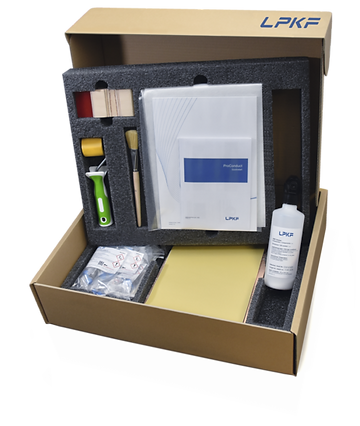
Processing Steps


Accessories and Options

Convection Oven
Used for curing ProConduct paste, pre-drying PCB surfaces before solder mask application, and curing solder mask or labels. It features precise temperature control and a timer, completing processes in around 30 minutes for efficient workflow support.
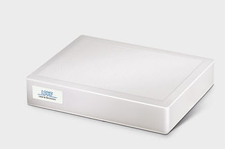
Vacuum Table
Keeps the workpiece flat across the entire surface during processing, preventing substrate bending. It is especially useful for flexible and rigid-flex PCBs, enabling stable handling without the need for additional mechanical holding devices.
LPKF Contac S4 Tabletop Through-Hole Electroplating
A compact tabletop electroplating system designed for reliable multilayer PCB production, enabling safe and uniform through-hole connections without requiring chemical expertise, ideal for advanced in-house prototyping environments.
-
Galvanic Through-Hole Plating
Provides reliable electrical interconnection for multilayer PCBs using a six-bath cascade process. Ensures homogeneous copper deposition inside vias and supports boards up to eight layers with high structural integrity.
-
Uniform Copper Layer Formation
Uses optimised anode systems and reverse pulse plating to achieve consistent copper thickness across hole walls and surface layers, improving conductivity and long-term reliability.
-
Microvia Cleaning and Activation
Includes integrated cleaning and activation steps using air flow and black hole technology to ensure strong bonding between plated holes and surface copper.
-
Optional Tinning Process
A final tin bath can be applied to improve surface protection and enhance solderability, increasing durability during assembly and testing.
-
User-Friendly Operation
The touchscreen-guided interface simplifies operation, offering automatic process control, maintenance alerts, and pre-set parameters, removing the need for chemical handling knowledge.